
Multi-functional Release Layer
Applications
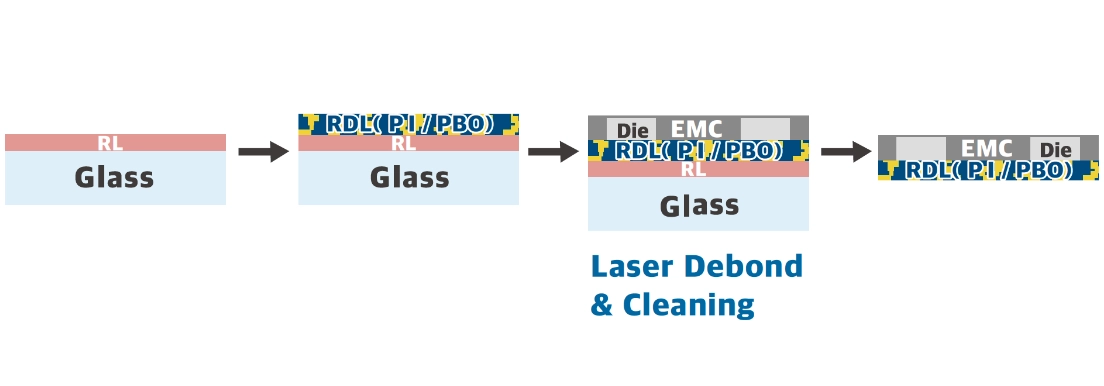
Temporary bonding of wafer to glass carrier has emerged as a viable method for various electronic device processing. Laser debonding enables the use of laser release layer (RL) that can withstand high temperatures above 300°C. The processed devices are finally debonded and separated from the carriers easily.
Features
- Excellent thermal resistance and stability over 300°C
- Easily stripped by laser
- Applicable under various laser wavelengths (308/355/532/1064nm) with high absorption
- Optical alignment(Tunable IR absorption or transmittance)
Specifications
| Product Name | LRA series | ||
|---|---|---|---|
| Features | High laser absorption efficiency | ||
| Laser Debond Wavelength |
| nm | 308~1064 |
| Clean Method | Plasma | ||
| Recommend Process Conditions | Coating Method | - | Slit Or Spin |
| Pre-bake | °C ; min | 90 ; 10 | |
| Post-bake | °C ; min | 250 ; 30 | |