
Redistribution Layer
Applications
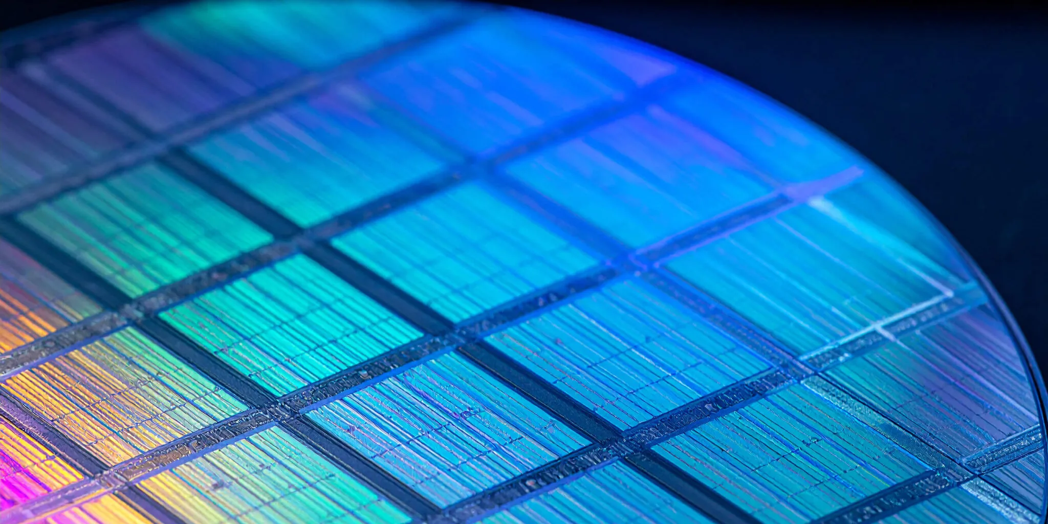
Varnish-type photosensitive dielectrics for the advanced chip packaging (WLP/PLP) are designed, which could be spin or slit-coated into thin film on the substrate and is photosensitive, able to be patterned into multi-layer redistribution layer (RDL). Low curing temperature, excellent Cu adhesion and electric properties are achieved for the varying chip applications.
Features of General Type
- Low temperature curing
- Excellent Cu adhesion
- Low CTE
- High resolution
- Excellent chemical resistance
Features of Low Dk/Df Type
- Low temperature curing
- Low Dk/Df
- High resolution
- Excellent chemical resistance
Specifications
| Product Name | PD series | |||||
|---|---|---|---|---|---|---|
| Features | .NMP free .Good mechanical properties | .NMP free .Low curing temp. | .NMP free .Low curing temp. .Low shrinkage | .NMP free .Low curing temp. .Higher modulus | .NMP free .Low curing temp. .Low Dk | |
| Development | Solvent | Solvent | Solvent | Solvent | Solvent | |
| Patterning | Negative | Negative | Negative | Negative | Negative | |
| Structure | Polyimide | Polyimide | Polyimide | Polyimide | Polyimide | |
| Curing temp./time | oC/time | 360/1h | 230/1h | 200/1h | 190/2h | 180/3h |
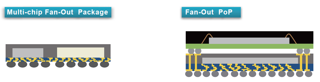
| Application Example | Buffer Coating Flip Chip | Fan-out | ||||