
Photosensitive Dielectric/Passivation

Applications
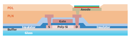
PBO dielectric layers can be used as the pixel defining layer (PDL) over the pixel electrode or the planarization layer (PLN) covering the TFTs in an organic light emitting diode display (OLED) and Electronic Paper Display (EPD).
| 
|
Features
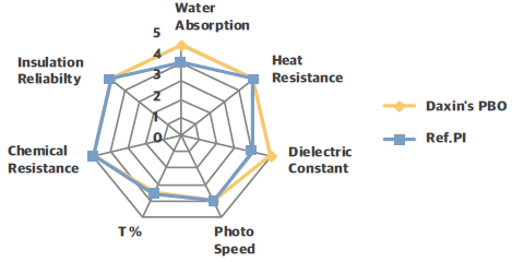
- Low water absorption
- Low dielectric constant
- Precision planarization capabilities
- Excellent mechanical and thermal properties
- High chemical resistance
- New : UV-resistance
Specifications
| Product Name | PDLN-200 Series | Remarks | |||
|---|---|---|---|---|---|
| Pattern Availability | PLN | PDL | PS | ||
| Features | THK 2.0µm | THK 1.5µm | THK 1.0µm | ||
| Water Absorption | % | (1)0.11 | TGA(RA85/85,24Hr) | ||
| Td(1%) | ℃ | 293 | |||
| Weight Loss | % | 0.57 | After250℃/1hr | ||
| Chemical Resistance | - | 5B | TMAH, Stripper, | ||
| Dielectric Constant | - | 3.43 | @1kHz | ||
| Recovery Ratio | % | 55.4 | Bump size: | ||
| Transmittance | % | 94.5 | THK1.5µm at | ||