
Product
Semiconductor Materials
Photosensitive Dielectric

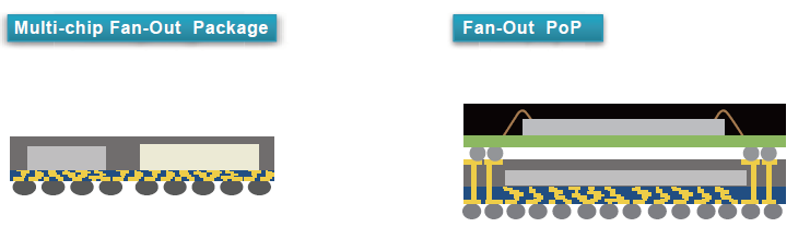
| Applications |
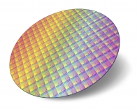
Varnish-type photosensitive dielectrics for the advanced chip packaging (WLP/PLP)are designed, which could be spin or slit-coated into thin film on the substrate and isphotosensitive, able to be patterned into multi-layer redistribution layer (RDL). It can also beapplied as a stress buffer coating. Low curing temperature, excellent Cu adhesion and electricproperties are achieved for the varying chip applications.
![]() Features
Features
- Low temperature curing
- Excellent Cu adhesion
- Low CTE
- Excellent chemical resistance
- High resolution
- Good electrical properties (Dk/Df)
![]() Specifications
Specifications
Please refer to our E-catalog.